

Kris purchased a new car so that the family could take a road trip. However, due to production disruptions, the vehicle has not been delivered for nearly a year, and he does not know when the wait will be over. In addition, a laptop, which he had ordered online for his children's online education, took two months to be delivered. It seems that this kind of story is not unique to Kris and his family as more and more people have similar experiences. So, what exactly is happening worldwide?
The root cause lies in the supply shortage of semiconductors. The supply chain bottleneck—triggered by COVID-19—has resulted in a worldwide semiconductor shortage. In 2021, when automobile production lines shut down due to the shortage, the semiconductor industry was put under an unprecedented spotlight. Also, as makers of smartphones, PCs, and home appliances also suffered semiconductor-shortage concerns, the interest surrounding supply chain issues and production disruptions led to more heated attention.
This can be seen in Google Trends, an index of keyword searches from Google. “Semiconductor shortage” appeared from the end of 2020, with the search for this phrase seeing an enormous number of hits in the second quarter of 2021. People have only recently realized that we live in a world of semiconductors since it was taken for granted in the past.
The boom in the semiconductor market due to rising demand for semiconductors is expected to continue for some time. In February of 2022, the U.S. Semiconductor Industry Association (SIA) announced that worldwide semiconductor chip sales in 2021 amounted to $555.9 billion—a record high and an increase of 26.2% from the previous year. The SIA noted that the industry is expected to show a growth rate of 8.8% in 2022 as semiconductor manufacturers invest in the construction of new factories to respond to market demand. In particular, as 4th industrial revolution technologies develop rapidly, the demand for high-performance semiconductors is expected to skyrocket as well. This is because, as the paradigm changes to a hyper-connected society, many smart products will be produced, and the performance of storing and processing data of these products must also be further enhanced. The expansion of 5G mobile communication, artificial intelligence (AI), autonomous driving, and cloud computing, which are essential conditions for a hyper-connected society, will inevitably increase the demand for high-performance semiconductors.
The rising hero of semiconductor substrates
On the other hand, the improvement of semiconductor performance that can be achieved through microprocessing technology is nearing its limit. As a result, the industry is focusing on the added value ushered in by technological innovation of the packaging process, a semiconductor post-processing technology, as interest in semiconductor package substrates increases.
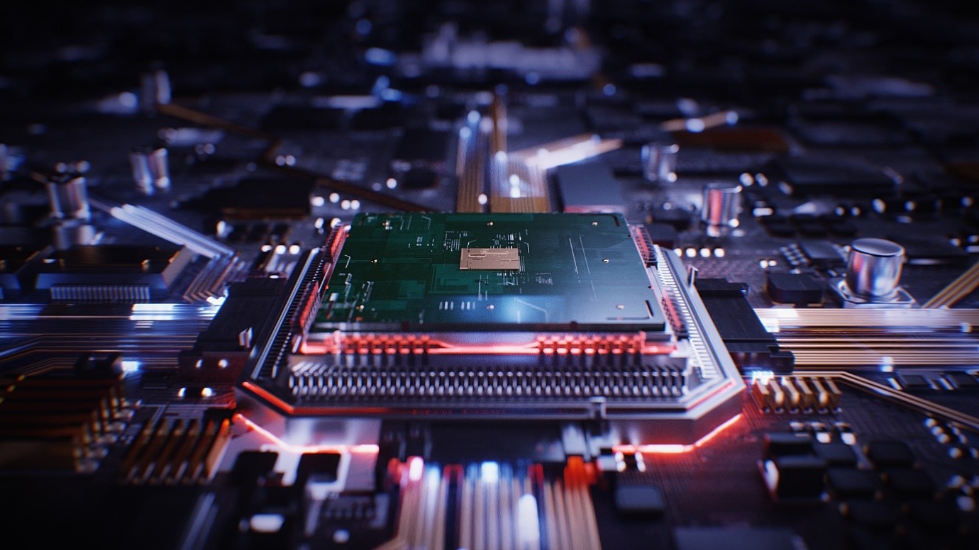
A semiconductor-package substrate is a circuit-connection component that electrically connects and mechanically supports the semiconductor chip to the main board. It is used not only in home appliances such as TVs and refrigerators, but also in all products that use semiconductors, such as smartphones, automobiles, and airplanes. Among them, the flip chip ball grid array, or FC-BGA, is a high-integration package substrate used to connect high-density semiconductor chips to the main board and is regarded as a new growth engine among semiconductor package substrates.
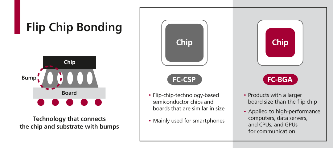
<Flip-chip bonding technology>
Technology that connects the semiconductor chip and substrate is evolving from wire-bonding technology that uses fine wires, to the wireless flip-chip method that uses bumps for package size reduction and faster electrical connections. The flip-chip method is a technology that flips down the active area of a chip and attaches it to another substrate or chip, while connecting the chip to the substrate by making ball-shaped bumps with solder, copper, nickel, and gold. Substrates manufactured with flip-chip technology are largely divided into Flip Chip-Chip Scale Package (FC-CSP) and FC-BGA; FC-CSP is used mostly in smartphones, while FC-BGA is applied in high-performance computers, data servers, and CPUs/GPUs for communication.
FC-BGA particularly has technical strengths in terms of area, density, and electrical signal transmission speed. It can respond to the increase in the size and area of high-performance processors, and by shortening the distance between the chip and the board, the number of input/output (I/O) terminals is increased to create a miniaturized form factor. Furthermore, the chip and board are directly connected with bumps, which leads to minimized electrical-signal-transmission pathways.
For this reason, FC-BGA is much more complex, requires advanced technology, and is used in products with high electrical-signal exchanges. Demand is increasing in various fields such as CPU/GPU for PCs, servers, semiconductors for communication devices, base stations, and System on Chips (SoCs) for vehicle electronic components. In particular, the supply shortage is expected to continue for some time as there are few companies with the technological capability, while demand is rapidly increasing due to wide-spread contactless communication and improved semiconductor performance.
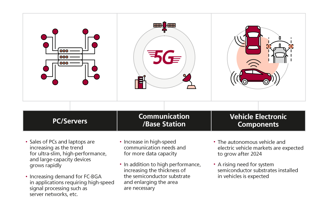
<FC-BGA main applications and market demand forecast>
LG Innotek fosters FC-BGA based on its expertise in RF-SiP and AiP technologies
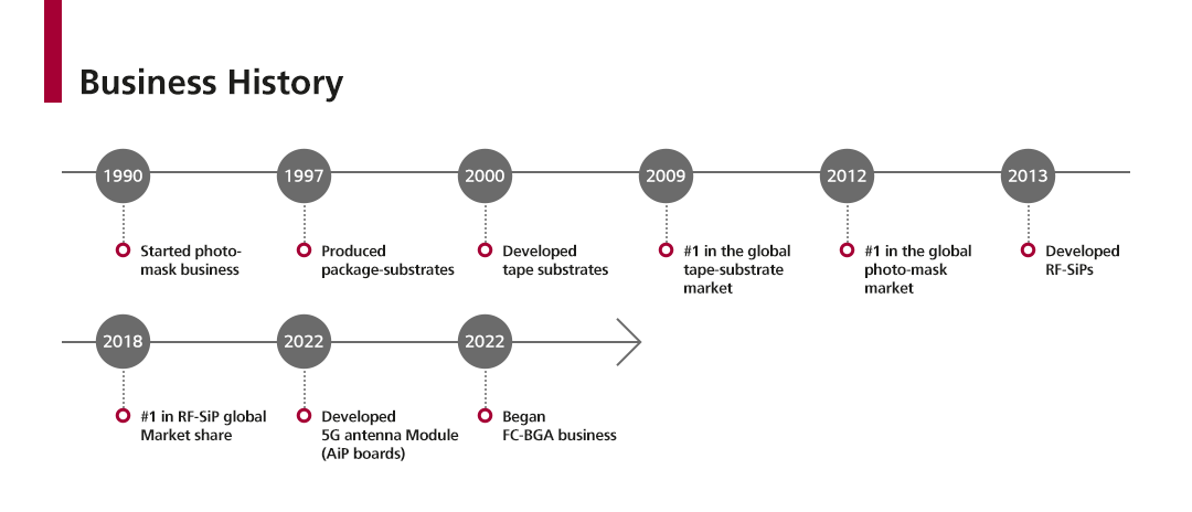
LG Innotek leads the semiconductor substrate market with technological innovation. The company already ranks No. 1 in the world in the semiconductor-substrate market for communications such as substrates for radio frequency package systems (RF-SiP) and 5G millimeter wave antenna packages (AiP). It is also demonstrating leadership in the field of FC-CSP substrates used in high-performance mobile-application processors (APs). Based on its world-class competitiveness in semiconductor-substrate technology, LG Innotek took the first step in expanding its FC-BGA business. Last year, a separate organization in charge of the FC-BGA business was newly established, and this February, a 413 billiion KRW (USD $340 million) investment plan in FC-BGA equipment and facilities was announced.
<LG Innotek leading the global semiconductor substrate market>
● Applying competitive advantage of the existing substrate-material business to new FC-BGA technology
In terms of materials and methods, various technological synergies can be expected by combining the strengths of the existing substrate-material business—recognized in the global market—to FC-BGA technology. For instance, LG Innotek’s RF-SiP and FC-CSP technologies for realizing high multi-layering and fine-patterning can be applied to this new technology.
● Preparing for the future with R&D capabilities
LG Innotek is beefing up its R&D investment and future technology development to respond to future high-performance semiconductors. In particular, to strengthen its FC-BGA competitiveness, the company is focusing on future technology research and development of advanced products for high-performance semiconductor substrates. These include core-layer-processing, micro-circuit, high-quality-plating, and simulation technologies, as well as material-processing technology that meets customer needs for communication, PCs, and servers.
● Digital twin & smart factories
LG Innotek has secured development and manufacturing competitiveness from digital innovation in the entire value chain, from product design to production. The digital twin-based R&D platform can dramatically shorten the lead time of customer product development by designing and verifying products virtually, and predicting and responding to possible defects in the customer's process in advance. In addition, by designing a factory through an AI/big data-based virtual process, the company is able to build a system that enables production with high initial yields with a reduced set-up period and can establish efficient operations through process and logistics automation.
With the contactless culture becoming part of everyday life, and the demand for IT products, the trend toward autonomous driving, and the construction of data centers on the rise, the number of essential technologies using semiconductors will increase in the future. The demand for FC-BGAs in PCs, servers, telecommunication applications, base stations, and automotive electronics is also expected to grow continuously. LG Innotek is committed to continuous customer-experience innovation by adding digital innovation to stable mass production, distribution capabilities and processing technology accumulated from its long business experience for various substrate products.

Related Articles

3D-Sensing Technology Brings the Metaverse to Life
Even More Real than Real Life

Connecting to Future Mobility
How Vehicle Communication Modules Are Leading the Autonomous-Driving Innovation Paradigm [PDF]

We are keeping an eye on your safety every moment
The Start of Innovation: Autonomous-Vehicle Camera Modules [PDF]
LG Innotek
E1/E3, 30, Magokjungang 10-ro, Gangseo-gu, Seoul, 07796, Republic of Korea
You are receiving this email because either you are a customer of LG Innotek or you have signed up to
receive marketing emails. If you received this in error, please unsubscribe.
Copyright © 2026 LG Innotek. All rights reserved.